

The latest speculation about AMD’s upcoming RDNA 5/UDNA architecture promises up to 96 compute units for gaming GPUs.
The rumor mill surrounding AMD’s upcoming GPU generation is picking up speed. Four chip designs have now been leaked, which are said to be intended for the next series of graphics cards.
In particular, the number of shader units is on the rise again after the RX 9000 did without a high-end model. However, the leaked data does not indicate any direct competition with Nvidia, at least not nominally.
Four chips in four sizes
The information comes from Kepler_L2, who is usually well informed on this subject, in Anandtech forum explained the four chip designs mentioned in more detail. Internally, at least, the variants are known as ”AT0,“ ”AT2,“ ”AT3,“ and ”AT4.”
- AT0 is the largest chip, with all other dies becoming smaller in descending order.
- If you’re wondering where AT1 has gone, this design has reportedly been canceled, as YouTuber “Moore’s Law is Dead” recently explained.
The top-of-the-line AT0 model therefore has 96 compute units (CUs). Below that is the AT2 design with 40 CUs for the performance segment, followed by AT3 with 24 CUs for mainstream applications and AT4 with 16 CUs as an entry-level option. All chips are to be manufactured based on the UDNA architecture.
Strategic architecture change
AMD announced last year that the end of the RDNA architecture was imminent.
It will be replaced by the “Unified DNA” strategy, the new UDNA generation, which combines gaming and data center architecture under one roof.
This consolidation is intended to reduce development costs and at the same time enable economies of scale in manufacturing, as you can see in the aforementioned gradation.
As usual, UDNA is also structured hierarchically.
As usual, UDNA also has a hierarchical structure, so to speak.
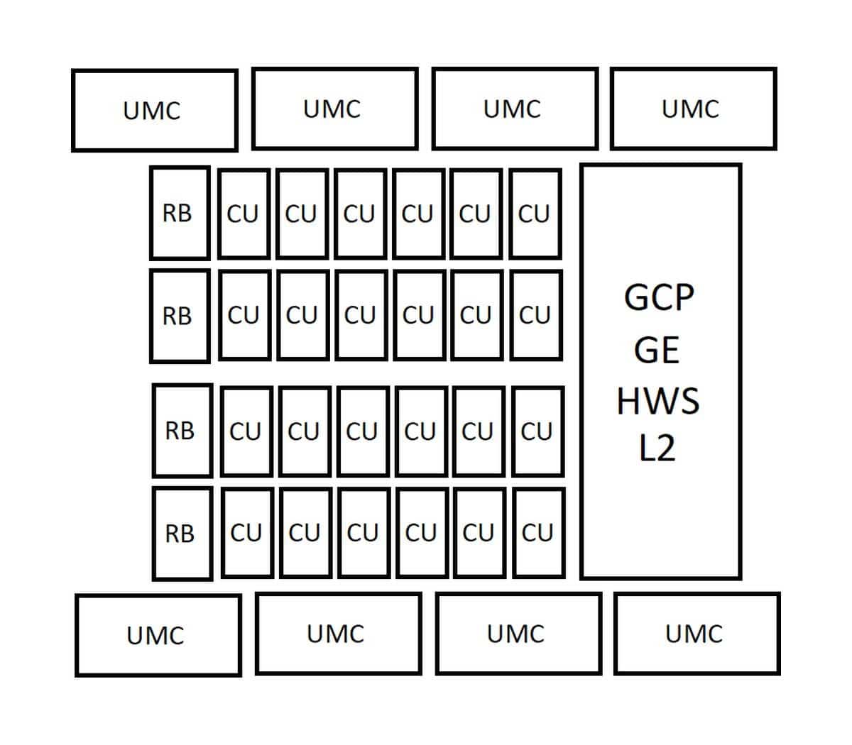
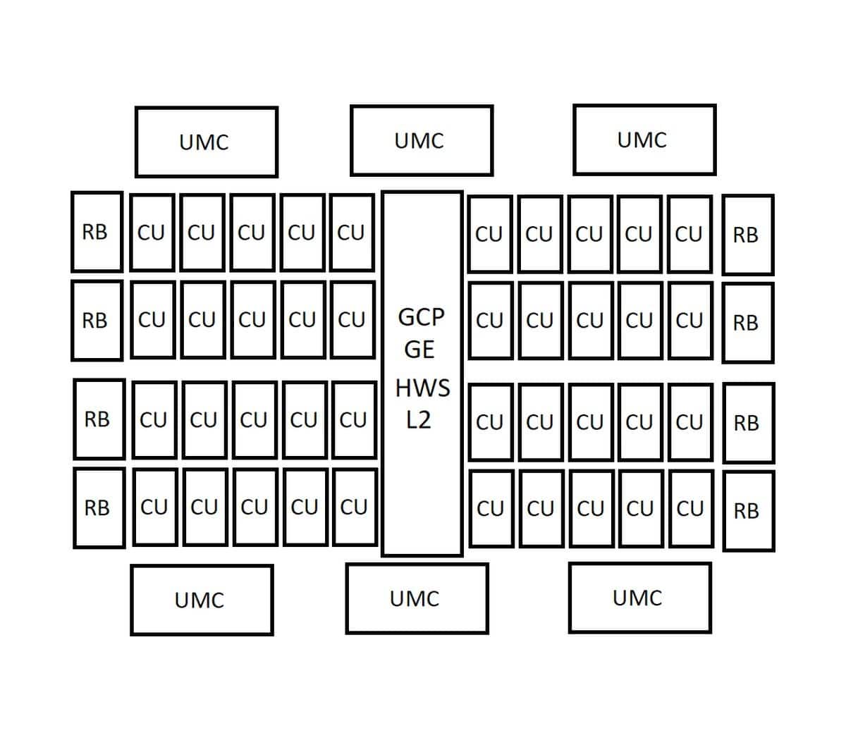
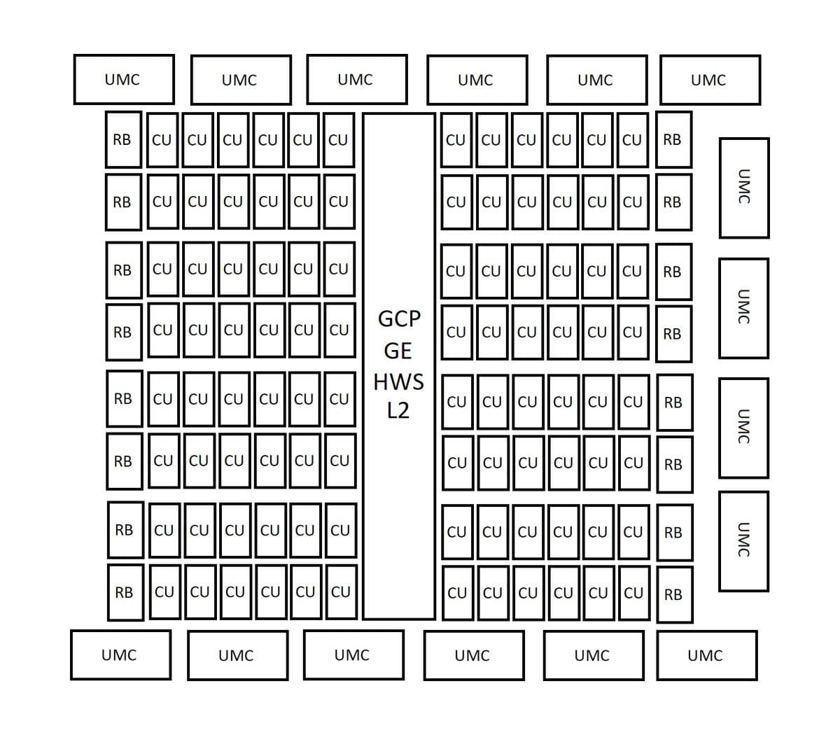
The AT0 chip contains a total of eight shader arrays, each with two shader engines. Each shader engine has six compute units, which results in the 96 CUs mentioned above in the example of the AT0 die.
The only exception here is that the AT2 chip is said to have only five CUs per shader engine, which explains the estimated 40 CUs.
The rough calculation for the number of shaders
If, as before, 64 shader units are installed per CU, we end up with a total of 6,144 shader units for the intended top model.
That would still be 50 percent more than the RX 9070 XT, but still far behind the RTX 5090 with 21,760 shader units. To a large extent, this is simply due to the “density” with which Nvidia packs its version of the CUs: there are 128 shader units per component here.
But even in a dream scenario where AMD actually uses 128 shader units per CU, you would only end up with 12,288 computing units – which would still be above the level of an RTX 5080.
Incidentally, according to the same calculation with 64 shader units per CU, the other chips end up with the following quantities:
- AT2: 2,560 shader units
- AT3: 1,536 shader units
- AT4: 768 shader units

AMD divides all dies into several categories
In this context, another change in strategy is imminent, as the leaker “Mareeswj” explains on the X platform. With the discontinuation of the aforementioned AT1 chip, which leaves a large gap in the planned UDNA portfolio, the end of “standalone gaming chips” seems to have arrived, at least for the time being.
AT0 will not only be used for Radeon graphics cards, but also for possible “prosumer” cards such as a Radeon VII.
- AT2, meanwhile, is intended for the next generation of classic consoles. Both the Xbox Next and the PlayStation 6 will once again feature AMD technology.
- The very small AT3 and AT4, on the other hand, are intended for tablets and handhelds.
As you can see, the current state of affairs is not exactly transparent. It will be some time before we learn anything more concrete: UDNA production is not expected to begin until the second quarter of 2026. This means that we are unlikely to get our hands on actual graphics cards until fall 2026 at the earliest.
